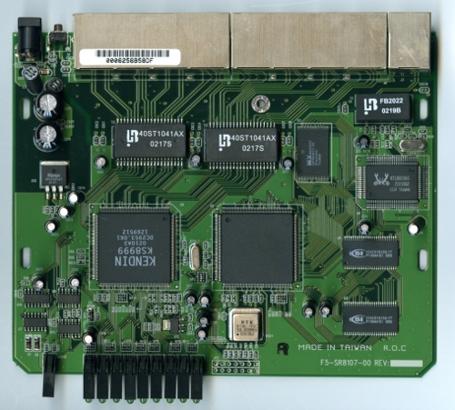
So I have two of these things at work and they go unused as the default firmware is somewhat lacking in features.
This made me wonder what the hardware looks like inside them. This is quite possibly one of the hardest pieces of hardware I’ve ever tried to open. The case isn’t sensible at all, but it seems if you can get the blue front section to decouple from the rest of it, it slides apart easily.
There’s one Samsung chip in the center that didn’t scan very well so here is what was written on that one:
SAMSUNG ARM 219B
S3C4510B01-QERO
SAMSUNG ARM 219B S3C4510B01 QERO Datasheet
Other chips:
KENDIN KS8999
0210A3
DC2953.0K1
1269512
2x 2MB SDRAM CHIP
SI
IC42S16100-7T
P1100441E1 0205
SI IC42S16100 2MB (16-MBIT) SDRAM Datasheet
RTL8019AS
23159Q2
213F TAIWAN
1MB FLASH RAM
MX M020832
29F800BTC-90
2F642400
TAIWAN
MX29F800T-B 1MB (8M-BIT) FLASH RAM Datasheet
HB 40ST1041AX
0217S
(Tiny black chip x4 at bottom left)
74HCT1230
E5687 14
Unn0215 D
74HCT125D
E2025 Q4
74HCT04D
AA361 27
Unn0214E
74HC14D
AA265 02
Unn0212F
Mainboard text:
MADE IN TAIWAN R.O.C.
F5-SR8107-00 REV: _______ (box left blank)
I think the conclusion we can come to here is that there is far too little flash and RAM to fit something like DD-WRT. I wonder what other projects might fit into these constraints?

The actual post is absolutely fantastic! A whole lot info as well as inspiration, both of which we all need! Like in order to appreciate the time and energy you place to your blog and more information you offer! I will bookmark your website!
Thanks for taking the time to fellate me. I’ve taken the liberty of removing your spam links from your comment, as surely that wasn’t your intent in posting here.
That’s a spambot…